Chapter II-Lesson 6 of 10 Transmission Lines - Wave Equations
Instructions
- Read the lecture (displayed below) [1 hour]
- Watch the video [12.38 minutes]
- Do the exercises [~30 minutes]
Total time = [~2:00 hours]
Lesson 6 of 10
: Transmission Lines - Wave Equations
The Issues of Reflections and Standing Waves
In this section, we investigate the issues with reflections and the resulting standing waves on transmission lines. To do that, we need to recognize that the purpose of a TL is to deliver the signal/power of the source/transmitter to the load/receiver end. Having said that, it is logical that a reflection from that end indicates the lack of a signal/power "full/adequate" delivery and that "some" of that signal/power was "denied/altered" and traveled back the "wrong" way. In terms of power, we can guess that more power could have been delivered to the load if none was reflected. Also, in terms of signal, the receiving end is not seeing the "one" signal that was intended but received multiple deliveries over time.
At this point, we need to demonstrate the concepts discussed above analytically, for both power and signal deliveries.
Power Delivery:
First, we need to understand the concept of power available from a source. To do so, let us assume a simple source load arrangement as shown in Figure 2.18. We will carry the analysis in the frequency domain for the convenience of avoiding differential equation formation and solutions. After all, we will be "swimming close to the shore" as we have done earlier and maintain close ties with the physics involved.
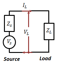
Figure 2.18
Figure 2.18
Now, let us evaluate the power delivered to the load in the simple source load circuit shown in the figure. The current in the load$~{{I}_{L}}={{V}_{s~}}/({{Z}_{s}}+{{Z}_{L}}$) and hence, the power delivered to the load is given by:
${{P}_{L}}={{\left| {{I}_{L}} \right|}^{2}}\cdot Re\left[ {{Z}_{L}} \right]\tag{2.63}$
Using the notations ${{Z}_{s}}={{R}_{s}}+j{{X}_{s}}$ and ${{Z}_{L}}={{R}_{L}}+j{{X}_{L}}$ where ${{R}_{s}}$, ${{X}_{s}}$, ${{R}_{L}}$, and ${{X}_{L}}$ are the resistive and reactive parts of the source and load impedances, respectively, we can rewrite the expression in Equation (2.63) as follows:
${{P}_{L}}={{\left| {{V}_{s}} \right|}^{2}}\frac{\left[ {{R}_{L}} \right]}{\left[ {{\left( {{R}_{s}}+{{R}_{L}} \right)}^{2}}+{{\left( {{X}_{s}}+{{X}_{L}} \right)}^{2}} \right]}$
This power is maximum when the following conditions are BOTH met:
${{X}_{s}}+{{X}_{L}}=0~and~{{R}_{s}}={{R}_{L}},~which~means~{{Z}_{L}}=Z_{s}^{*}\tag{2.64}$
The reactance condition is simply telling us that the load reactance should null out (tune out) that of the source (or vice versa). So, we learn that in power transmission, since most of the loading (homes, factories, etc.) is inductive (motors, appliances, etc.), the load reactance is inductive and hence a capacitive source impedance is necessary to improve power delivery to these loads. This typically is referred to as capacitive power factor correction.
With tuned out reactances, the second condition signifies that the resistive components of the source and load must be matched to each other, ${{R}_{s}}={{R}_{L}}$.
With both constraints met, the power delivered to the load is the maximum power possible to obtain from the source and hence the term power available, ${{P}_{av}}$
${{\text{P}}_{\text{av}}}={{\left[ {{\text{P}}_{\text{L}}} \right]}_{\text{max}}}=\frac{{{\left| {{\text{V}}_{\text{s}}} \right|}^{2}}}{4{{\text{R}}_{\text{s}}}}\tag{2.65}$
Now, how does this apply to our TL network? First, for the source to deliver its "maximum" available power, the impedance seen by the source (${{Z}_{in}}=Z\left( 0 \right)$) is the loading impedance to the source. Hence, the requirement becomes:
$\text{Z}_{\text{s}}^{\text{*}}={{\text{Z}}_{\text{in }}}~\overset{\text{yields }}{\mathop{\to }}\,\text{ }\!\!\Gamma\!\!\text{ }_{\text{s}}^{\text{*}}={{\text{ }\!\!\Gamma\!\!\text{ }}_{\text{in}}}={{\text{ }\!\!\Gamma\!\!\text{ }}_{\text{L}}}\cdot {{\text{e}}^{-2\text{ }\!\gamma\!\text{ }\ell }}\tag{2.66}$
Likewise, for the line to deliver maximum power to the load, the condition is:
$\text{ }\!\!\Gamma\!\!\text{ }_{\text{L}}^{\text{*}}={{\text{ }\!\!\Gamma\!\!\text{ }}_{\text{s}}}\cdot {{\text{e}}^{-2\text{ }\!\gamma\!\text{ }\ell }}~\overset{\text{ yields }}{\mathop{\to }}\,\text{ }\!\!\Gamma\!\!\text{ }_{\text{s}}^{\text{*}}={{\text{ }\!\!\Gamma\!\!\text{ }}_{\text{L}}}\cdot {{\left[ {{\text{e}}^{2\text{ }\!\gamma\!\text{ }\ell }} \right]}^{\text{*}}}\tag{2.67}$
Comparing the two conditions, we find out that both conditions can be simultaneously satisfied if and only if$~{{e}^{-2\!~\gamma ~\!\ell }}={{\left[ {{e}^{2\!~\gamma ~\!\ell }} \right]}^{*}}$, which can only be true for lossless lines only, $\alpha =0.$
Signal Delivery:
In this section, we will discuss the effect of multiple reflections (and hence the standing waves) on the quality (fidelity) of signal delivery. This is of prime concern in communication applications of TLs. For the receiving end not to get the "full" delivery of the transmitted signal and having to "reflect" part of it could be thought of as a reduction in the level of the received signal. The fact of the matter is that it can go beyond affecting the level to actually causing distortion to the received signal.
If we examine the expression for the receiving end signal, Equation (2.58), we can see that the relationship between ${{V}_{L}}$ and ${{V}_{S}}$ includes, in general, complex coefficients. This implies that the signal arriving at the receiving end suffers both amplitude and phase changes. Typically, this is of no concern for single harmonic transmission applications. However, for communication applications, where a composite signal with components of multiple frequencies are propagated on the line, signal components of differing frequencies are expected to have different amplitude and phase modifiers.
The same can be said regarding digital communications where the information signal is coded in pulse format. These "time domain" pulses are rich in harmonics and thus contain a wide spectrum of frequencies. If the frequency components are to experience different "treatment" as they travel from the source to the load, the arrival composite of altered frequency components would result in "distorted" pulses, thus compromising the quality and fidelity of the signal delivery. This form of "pulse" distortion is called pulse spreading or "dispersion".
In addition to pulse spreading as discussed, multiple reflections result in multiple arrivals of time domain signals at the receiving end; see Figure 2.17. An example of this issue is demonstrated in Figure 2.19. In this example, a single pulse transmission on a line with multiple reflections is shown. The receiving end signal does not arrive to the load all at once; instead, the load receives multiple arrivals at different delay times. Therefore, the arrival at the receiving end is spread over an extended period due to the multiple occurrences in the time domain.
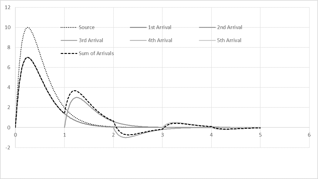
Figure 2.19
Figure 2.19
One obvious consequence is the serious limitation this form of dispersion causes to digital communication applications. The rate of sending information pulses has to be slowed down to allow adequate decay of the multiple reflections of one pulse before sending the next one.
Ideally, for communication purposes where the fidelity reception of the transmitter signal is very important, multiple reflections are undesirable. To eliminate multiple reflections, either ${{\Gamma }_{s}}$ or ${{\Gamma }_{L}}$ (or both) should be reduced to zero. Hence, according to Equation (2.58),
$\left\{ \begin{matrix}
{{\Gamma }_{s}}=0~~~\overset{\text{ yields }}{\mathop{\to }}\,~~{{V}_{L}}=\left\{ \frac{{{V}_{s}}~}{2} \right\}\left( 1+{{\Gamma }_{L}} \right)~{{e}^{-\!~\gamma ~\!\ell }} \\
{{\Gamma }_{L}}=0~~~\overset{\text{ yields }}{\mathop{\to }}\,~~{{V}_{L}}=\left\{ \frac{{{V}_{s}}~}{2} \right\}\left( 1-{{\Gamma }_{s}} \right)~{{e}^{-\!~\gamma ~\!\ell}} \\{\!\!\!\!\!\!\!\!\!\!{\Gamma }_{s}}={{\Gamma }_{L}}=0~~~\overset{\text{ yields }}{\mathop{\to }}\,~~{{V}_{L}}=\left\{ \frac{{{V}_{s}}~}{2} \right\}~{{e}^{-\!~\gamma ~\!\ell }} \\
\end{matrix} \right.\tag{2.68}$
Furthermore, for signal fidelity, all frequency components of ${{V}_{L}}$ should have the same propagation treatment as they travel from the source to the load. In other words, ${{V}_{L}}/{{V}_{S}}$ should be frequency independent. Assuming ${{e}^{-\!~\gamma ~\!\ell }}$ of the transmission line to produce the same signal delay for all frequencies, we add further constraints to the above requirements as follows:
$\left\{ \begin{matrix}
{{\Gamma }_{s}}=0~~~\overset{\text{ yields }}{\mathop{\to }}\,~~{{V}_{L}}=\left\{ \frac{{{V}_{s}}~}{2} \right\}\left( 1+{{\Gamma }_{L}} \right)~{{e}^{-\!~\gamma ~\!\ell }}- Fidelity~constraint: {{\Gamma }_{L}}~should~be~real \\
{{\Gamma }_{L}}=0~~~\overset{\text{ yields }}{\mathop{\to }}\,~~{{V}_{L}}=\left\{ \frac{{{V}_{s}}~}{2} \right\}\left( 1-{{\Gamma }_{s}} \right)~{{e}^{-\!~\gamma ~\!\ell }}- Fidelity~constraint: {{\Gamma }_{s}}~should~be~real\\ {\!\!\!\!\!\!\!\!\!\!\!\!\!\!\!\!\!\!\!\!\!\!\!\!\!\!\!\!\!\!\!\!\!\!\!\!\!\!\!\!\!\!\!\!\!\!\!{\Gamma}_{s}}={{\Gamma}_{L}}=0~~~\overset{\text{ yields }}{\mathop{\to }}\,~~{{V}_{L}}=\left\{ \frac{{{V}_{s}}~}{2} \right\}~{{e}^{-\!~\gamma ~\!\ell }}- Fidelity~constraint: none \\
\end{matrix} \right.\tag{2.69}$
The requirements for signal fidelity can be summarized as follows: either ${{\Gamma }_{S}}~=~0$ or ${{\Gamma }_{L}}~=~0$, while the non-zero one should be real.
Combined Power and Signal Delivery Constraints:
According to the conditions in Equations (2.66) and (2.67), if either ${{\Gamma }_{S}}$ or ${{\Gamma }_{L}}$ is zero, the other should be zero as well. Hence, to combine the two sets of requirements for maximum available power delivered to the load while maintaining signal fidelity, we need to have both ${{\Gamma }_{S}}$ and ${{\Gamma }_{L}}$ equal to zero, meanwhile, we should be using a lossless (or near lossless) TL.
In practical cases, we can design the source to have a matching internal impedance to the TL used and hence maintain ${{\Gamma }_{S}}$ as zero. However, in many applications, we may not have control over the load impedance and consequently ${{\Gamma }_{L}}$. In such cases, a matching network becomes necessary to be implemented in order to enable the source-TL matched network to see an "equivalent" matched load. This will be discussed in detail in Addendum B: Impedance Matching.
Addendum B: Impedance Matching
How to Achieve Matching:
Referring to Figures 2.21 – 2.24, matching the load impedance to the source impedance implies making the projected load impedance at the source end equal to that of the source. In other words, making the input impedance of the load "network" equal the source impedance. It is worthy to mention here that although the discussion in this section is focused on matching the load to the source, the opposite is possible and doable through the same approaches presented here.
It is also important to cite that in typical practical cases, the source impedance is pure resistive, and hence that is what we will confine our discussion in this section to.
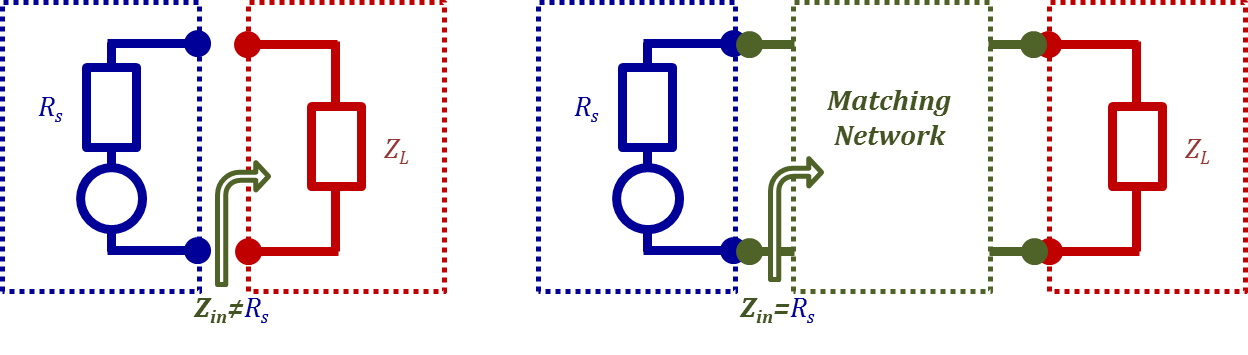
Figure 2.21
Figure 2.21
To bring the "projected" load impedance as viewed at the source port to the source impedance (resistance) value, a matching network is needed to act as an impedance transformer between the two values.
One may argue that a simple series or shunt impedance matching network would achieve the desired result, Figure 2.22. For example, if the load impedance (resistance) level is lower than that of the source then add a series impedance in the amount of ${{Z}_{series}={Z}_{s}-{Z}_{L}}$ thus making ${{Z}_{in}={Z}_{s}}$. On the other hand, if the load impedance (resistance) level is higher than that of the source, then add the matching network impedance in shunt, and hence ${{Z}_{in}={Z}_{L}}$ // ${{Z}_{shunt}}$ The problem with these configurations is that either ${{Z}_{series}~\text{or}~{Z}_{shunt}}$ are likely to contain resistive components and hence introducing loss elements to the circuit that would degrade its performance.
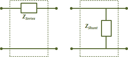
Figure 2.22
Figure 2.22
As the networks of Figure 2.22 prove inadequate, some of the typically used matching network forms are shown in Figures 2.23, 24, and 25.
L-PI-T Matching Networks:
Figure 2.23 shows three matching network configurations: the "L-section", the "$π$-network", and the "T-network".
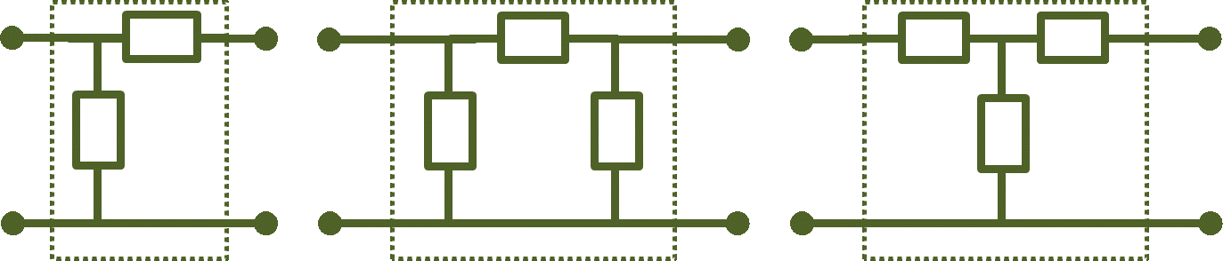
Figure 2.23
Figure 2.23
The literature has many references regarding the design approaches of such networks as well as comparisons of their performances. Depending on the network configuration, the design may be optimized in terms of bandwidth or other possible performance parameters.
For optimum performance, all matching network components must not add any loss to the circuit (or at least be "low loss" components).
In other words, the network elements need to be high quality "high-Q" reactances. Depending on the operating frequency of the circuit, discrete components cannot be used for lumped circuit elements sought in these networks as they may cause performance issues. If the size of the discrete components is not much smaller than the operating wavelength, as discussed earlier in Table (2.1), the component must be treated as a distributed "transmission line" device instead of a lumped element. Moreover, the physical devices for these elements will not be the pure reactive components sought in the design, as they will most certainly contain other parasitics.
Stub Matching:
At high frequencies, lossless transmission lines (or practically, low loss lines) are used instead of discrete components. Typical transmission line matching networks are shown in Figures 2.24-25. The design principle of the networks shown is to use a transmission line on the load side with the proper line parameters that would project a resistive value at its input port so that it would match the resistive values of the source impedance. Tuning reactances can then be added to achieve the desired full impedance match.
To further explain, assume we are working with the top configuration of Figure 2.24. We will need to choose TL parameters ${{R}_{o,ms}, {β}_{ms}}$, and ${{d}_{ms}}$ such that the real part of (${{Z}_{d}}$ = ${{Z}_{in,ms}}$) is equal to ${{R}_{s}}$. Using Equation (2.72), we can write:
$Real~part~of\left\{ {{Z}_{d}}={{R}_{o,ms}}\frac{\left[ {{Z}_{L}}~+~{{R}_{o,ms}}~\cdot ~ j\tan \left( {{\beta }_{ms}}~{{d}_{ms}} \right) \right]}{\left[ {{R}_{o,ms}}~+~{{Z}_{L}}~\cdot ~ j\tan \left( {{\beta }_{ms}}~{{d}_{ms}} \right) \right]} \right\}={{R}_{s}}\tag{2.76}$
The added series reactance $± {{j} {X}_{series}}$ is to tune out the imaginary part (reactance) of ${{Z}_{d}}$, and hence
$\pm j{{X}_{series}}+Imaginary~part~of\left\{ {{Z}_{d}}={{R}_{o,ms}}\frac{\left[ {{Z}_{L}}~+~{{R}_{o,ms}}~\cdot ~ j~tan\left( {{\beta }_{ms}}~{{d}_{ms}} \right) \right]}{\left[ {{R}_{o,ms}}~+~{{Z}_{L}}~\cdot ~ j\tan \left( {{\beta }_{ms}}~{{d}_{ms}} \right) \right]} \right\}=0\tag{2.77}$
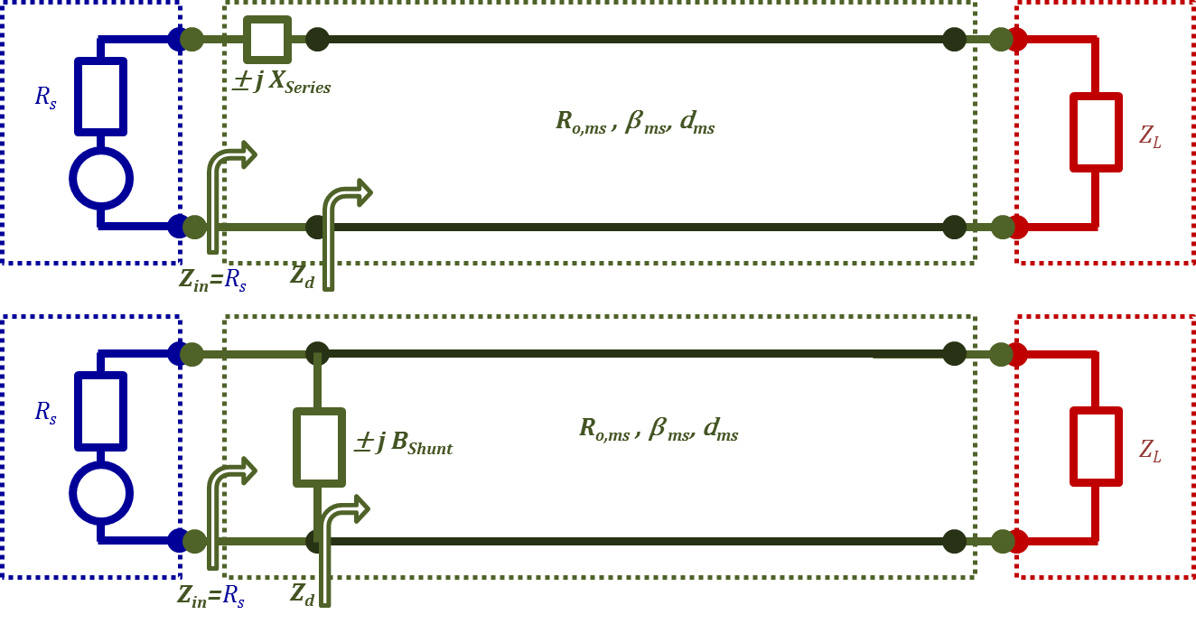
Figure 2.24
Figure 2.24
Similarly, the equations for the bottom configuration with the shunt reactance can be written in terms of the conductance and susceptance terms instead of resistance and reactance terms; hence,
$\text{Real }\!~\!\text{ part }\!~\!\text{ of}\left\{ {{\text{Y}}_{\text{d}}}={{\left[ {{\text{R}}_{\text{o},\text{ms}}}\frac{\left[ {{\text{Z}}_{\text{L}}}~+~{{\text{R}}_{\text{o},\text{ms}}}~\cdot ~\text{j }\!~\!\text{ tan}\left( {{\text{ }\!\beta\!\text{ }}_{\text{ms}}}~{{\text{d}}_{\text{ms}}} \right) \right]}{\left[ {{\text{R}}_{\text{o},\text{ms}}}\text{ }\!~\!\text{ }+\text{ }\!~\!\text{ }{{\text{Z}}_{\text{L}}}~\cdot ~ \text{j }\!~\!\text{ tan}\left( {{\text{ }\!\beta\!\text{ }}_{\text{ms}}}~{{\text{d}}_{\text{ms}}} \right) \right]} \right]}^{-1}} \right\}={{\left[ {{\text{R}}_{\text{s}}} \right]}^{-1}}\tag{2.78}$
and an added shunt susceptance $±{{j}{B}_{shunt}}$ is to tune out the imaginary part (susceptance) of ${{Y}_{d}}$; therefore,
$\pm \text{j}{{\text{B}}_{\text{shunt}}}+\text{Imaginary }\!~\!\text{ part }\!~\!\text{ of}\left\{ {{\text{Y}}_{\text{d}}}={{\left[ {{\text{R}}_{\text{o},\text{ms}}}\frac{\left[ {{\text{Z}}_{\text{L}}}~+~{{\text{R}}_{\text{o},\text{ms}}}~\cdot ~ \text{j}\tan \left( {{\text{ }\!\beta\!\text{ }}_{\text{ms}}}~{{\text{d}}_{\text{ms}}} \right) \right]}{\left[ {{\text{R}}_{\text{o},\text{ms}}}\text{ }\!~\!\text{ }+\text{ }\!~\!\text{ }{{\text{Z}}_{\text{L}}}~\cdot ~\text{j }\!~\!\text{ tan}\left( {{\text{ }\!\beta\!\text{ }}_{\text{ms}}}~{{\text{d}}_{\text{ms}}} \right) \right]} \right]}^{-1}} \right\}=0\tag{2.79}$
To realize the series reactance or shunt susceptance needed in the matching networks of Figure 2.24, series and parallel transmission line "stubs" as shown in Figure 2.25 are utilized. The idea is that an open- or short-circuited transmission line at one of its ends presents a pure reactive/susceptive input impedance at the other end; refer back to Table (2.2).
Typically, a short-circuited stub is used instead of an open-circuited one to avoid open-end radiation and associated losses at the open end of the line.
For a short-circuited stub, the corresponding parameters are to be chosen so that (using Equation (2.72) with ${{Z}_{L}}=0$).
for the series stub: $\pm {j}~{{\text{X}}_{\text{series}}}={j }\!~\!\text{ }{{\text{R}}_{\text{o},\text{st}}}\cdot \text{ }\!\!~\!\!\text{ tan}\left( {{\text{ }\!\!\beta\!\!\text{ }}_{\text{st}}}{{\text{d}}_{\text{st}}} \right)\tag{2.80}$
and, for the shunt stub: $\pm {j}~{{\text{B}}_{\text{shunt}}}={{\left[ {j }\!~\!\text{ }{{\text{R}}_{\text{o},\text{st}}}\cdot \text{tan}\left( {{\text{ }\!\!\beta\!\!\text{ }}_{\text{st}}}{{\text{d}}_{\text{st}}} \right) \right]}^{-1}}\tag{2.81}$
If an open stub is preferred, the equations for the stub reactances can be obtained for Equation (2.56) by setting ${{Z}_{L}}$ to $∞$ (or an estimate to its physical value). The results would be
for the series stub: $\pm {j}~{{\text{X}}_{\text{series}}}=-\text{ }\!~\!{ j }\!~\!\text{ }{{\text{R}}_{\text{o},\text{st}}}\cdot \text{ }\!\!~\!\!\text{ cot}\left( {{\text{ }\!\!\beta\!\!\text{ }}_{\text{st}}}{{\text{d}}_{\text{st}}} \right)\tag{2.82}$
and, for the shunt stub: $\pm {j}~{{\text{B}}_{\text{shunt}}}={{\left[ -\text{ }\!~\!{ j }\!~\!\text{ }{{\text{R}}_{\text{o},\text{st}}}\cdot \cot \left( {{\text{ }\!\!\beta\!\!\text{ }}_{\text{st}}}{{\text{d}}_{\text{st}}} \right) \right]}^{-1}}\tag{2.83}$
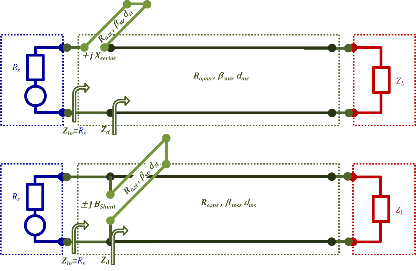
Figure 2.25
Figure 2.25
Later in this chapter, we will introduce the famous transmission line graphical technique known as the Smith Chart. This technique will be demonstrated to not only produce relatively simple computational solutions to transmission line problems, but also provide physical insight into the solution and the different parameters involved. As an application to the Smith chart, we will do the transmission line matching networks discussed above.
The Quarter Wave Transformer as a Matching Network:
In some special cases, a quarter wave transmission line section can be used to provide the desired matching between the source and the load.
Using Equation (2.72) again and setting $d~=~$λ$/~4$, we can write:
${{\text{Z}}_{\text{in}}}=\frac{{{\text{R}}_{\text{o}}}^{2}}{{{\text{Z}}_{\text{L}}}}\tag{2.84}$
The resulting projected impedance ${{\text{Z}}_{\text{in}}}$ is to be equated to $Rs$ for matching with the source impedance (resistance); hence,
${{\text{R}}_{\text{s}}}=\frac{{{\text{R}}_{\text{o}}}^{2}}{{{\text{Z}}_{\text{L}}}}$
which implies that $Z_L$ should be real. In other words, a lossless/low-loss quarter wave transformer is good for matching real (resistive) load impedances to resistive source impedances provided that we choose the characteristic impedance of the quarter wave section to be
${{\text{R}}_{\text{o}}}=\sqrt{{{\text{R}}_{\text{s}}}\cdot {{\text{R}}_{\text{L}}}}\tag{2.85}$
Figure 2.26 demonstrates the use of a λ$/4$ section for matching purposes.
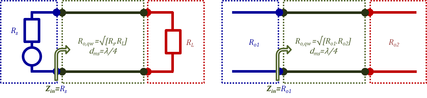
Figure 2.26
Figure 2.26
The Half Wave Transformer as a Matching Network:
Now, we wonder, what can a half wavelength section be used for ? Can it be used for matching as well ? The answer starts by using Equation (2.72) while setting $d~=~$λ$/2$, which yields:
${{Z}_{in}}={{Z}_{L}}\tag{2.86}$
which is independent of ${{R}_{o}}~$(the characteristic impedance of the half wave section). This means that the load must be already matched to the source, which may lead us to think that the λ$/2$ section has no practical use in matching problems.
Well, let us consider the case where a matched source and load pair must be connected, for some practical reason, by a TL whose characteristic impedance is different. In such case, a λ$/2$ section of this connecting line would be the ideal length, as it would maintain the existing matching between the source and the load. Such cases exist in real life where connecting transmission line sections must take a non-uniform shape such as a bent or a twist, etc.
These sections need to be designed to have a half wavelengths in order to maintain matching, see Figure 2.27.
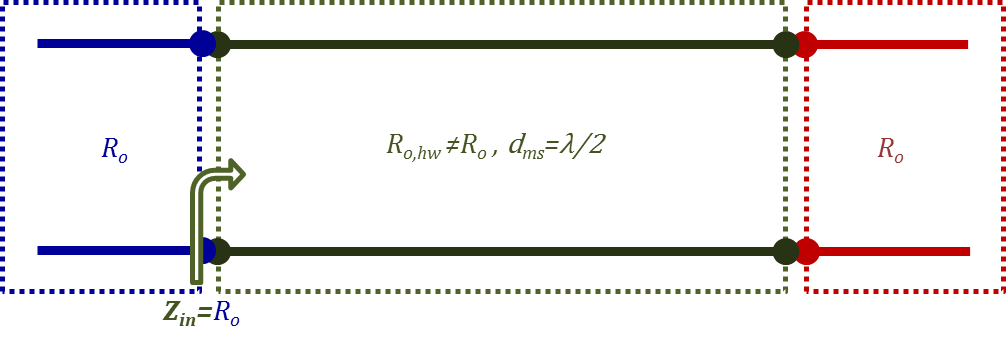
Figure 2.27
Figure 2.27
- Mention two undesirable effects that result from signal reflections.
- Referring to the circuit of Figure 2.18, what is the maximum power that can be delivered from a source voltage $V_s={2~Volts}$ and having internal impedance of $Z_s=50~Ohm$. What is the value of the voltage at the load in this case?
- What condition needs to be satisfied by the characteristic impedance of a TL so that the maximum power can be transmitted through it from a source?
- For a TL circuit where source impedance is matched to the characteristic impedance of the TL, what should the load value be to avoid harmonic distortion?
Return to Lesson
Return to Video
Examples II.6
- For the circuit shown in Figure 2.18 and having the following parameters: $V_s={2~Volts}$, ${{Z}_{s}}=50~Ohm$,$Z_o=50~Ohm$, and ${{Z}_{L}}=10~Ohm$. Find the power delivered to the load. What is the efficiency of the power delivery?
- In the above example, if the voltage source is replaced with a digital pulse signal source, will the signal be transmitted with perfect fidelity? Why or why not?
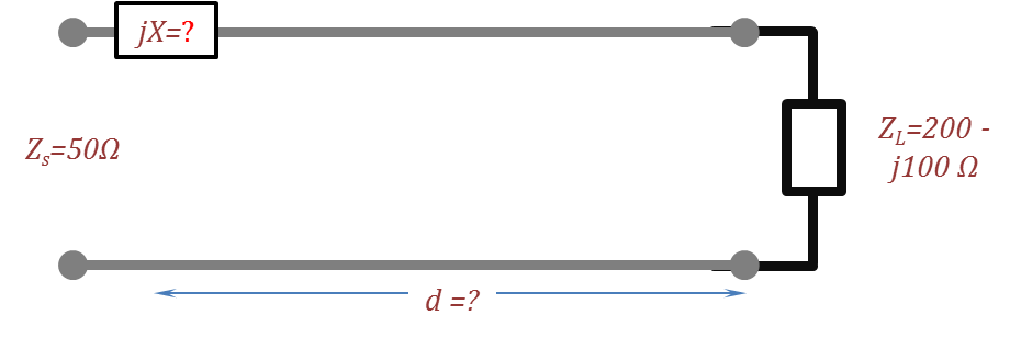
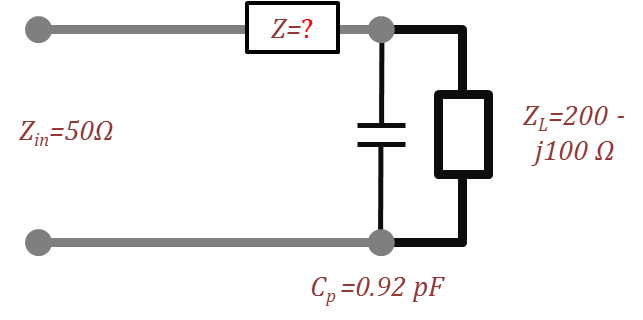
- For the circuit shown in the following figure, an L-section matching circuit is used. Find the impedance of the series impedance in the L-section that results in maximum power delivery.
Return to Lesson
Return to Video
Problems II.6
- For the circuit shown in fig 2.18 and having the following parameters: $V_s={2~Volts}$, ${{Z}_{s}}=50~Ohm$, $Z_o=50~Ohm$, and ${{Z}_{L}}=10~Ohm$. Find the power delivered to the load. What is the efficiency of the power delivery?
- For the same circuit in the above problem, plot the magnitude of the voltage at the load for frequencies in the range $100~MHz-10~GHz$. If the source generates a harmonically rich/wideband signal will it be distorted or not ? Explain.
- For the circuit shown in the figure below, find the length of the section of the TL (in fractions of λ )
and the series reactance that will result in maximum power delivery from a source having an internal resistance of $50~Ohm$. The characteristic impedance of the TL is $50~Ohm$.